Electron microscopy techniques | Electron beam

Scanning transmission electron microscopy

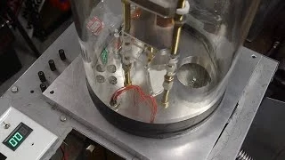
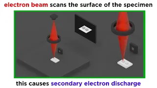
A scanning transmission electron microscope (STEM) is a type of transmission electron microscope (TEM). Pronunciation is [stɛm] or [ɛsti:i:ɛm]. As with a conventional transmission electron microscope (CTEM), images are formed by electrons passing through a sufficiently thin specimen. However, unlike CTEM, in STEM the electron beam is focused to a fine spot (with the typical spot size 0.05 – 0.2 nm) which is then scanned over the sample in a raster illumination system constructed so that the sample is illuminated at each point with the beam parallel to the optical axis. The rastering of the beam across the sample makes STEM suitable for analytical techniques such as Z-contrast annular dark-field imaging, and spectroscopic mapping by energy dispersive X-ray (EDX) spectroscopy, or electron energy loss spectroscopy (EELS). These signals can be obtained simultaneously, allowing direct correlation of images and spectroscopic data. A typical STEM is a conventional transmission electron microscope equipped with additional scanning coils, detectors, and necessary circuitry, which allows it to switch between operating as a STEM, or a CTEM; however, dedicated STEMs are also manufactured. High-resolution scanning transmission electron microscopes require exceptionally stable room environments. In order to obtain atomic resolution images in STEM, the level of vibration, temperature fluctuations, electromagnetic waves, and acoustic waves must be limited in the room housing the microscope. (Wikipedia).

Scanning transmission electron microscopy
Video thumbnail

DIY Scanning Electron Microscope - Overview

Today, I finally produced an image with my DIY scanning electron microscope. I've spent the last few months working on this project, and am encouraged by today's success. There is still a lot of work left to do in making the image higher resolution, and eliminating sources of noise, howe

From playlist Scanning Electron Microscope

Video thumbnail

Electron beam control in a scanning electron microscope

I describe electron beam optics and deflection as they are employed in scanning electron microscopy. http://web.jfet.org/vclk/ - Deflection amplifier http://www.johngineer.com/blog/?p=648 - CRT Christmas tree http://www.fei.com/ - FEI Company

From playlist Scanning Electron Microscope

Video thumbnail

DIY Scanning Electron Microscope - Tektronix contest entry

Vote for me here: http://mytektronixscope.com/videos/ I am using my Tektronix 2246 analog oscilloscope to show the image generated by my DIY electron microscope. The 2246 is operating in X-Y mode, with the channels connected to a raster scan generator. The vertical scanning frequency

From playlist Scanning Electron Microscope

Video thumbnail

DIY Scanning Electron Microscope - Operation procedure

After getting back from Maker Faire (which is always a hugely enjoyable and inspiring event), I thought that my microscope might need some repairs. As it turned out, I only had to change the filament and tighten some screws that came loose during the trip back from the Faire. The microsc

From playlist Scanning Electron Microscope

Video thumbnail

Electron Microscopy (TEM and SEM)

We've talked a lot about light microscopy, but this technique has inherent limitations in resolution and magnification. The next paradigm in microscopy that emerged in the middle of the 20th century was electron microscopy. Because electrons have much shorter wavelengths than photons, elec

From playlist Microbiology/Infectious Diseases

Video thumbnail

DIY Scanning Electron Microscope - Sources, Costs and References

Please visit my blog post to see the references and sources for this project: http://benkrasnow.blogspot.com/2011/03/diy-scanning-electron-microscope_26.html

From playlist Scanning Electron Microscope

Video thumbnail

DIY Scanning Electron Microscope - Electron Gun Detail

I explain the detailed operation of the electron gun in my DIY scanning electron microscope project.

From playlist Scanning Electron Microscope

Video thumbnail

Peng Wang - Electron Ptychography: Emerging Computational Microscopy for Physical/Biological Science

Recorded 28 October 2022. Peng Wang of the University of Warwick presents "Electron Ptychography: An Emerging Computational Microscopy for Physical and Biological Sciences" at IPAM's Mathematical Advances for Multi-Dimensional Microscopy Workshop. Abstract: Ptychography is an emerging comp

From playlist 2022 Mathematical Advances for Multi-Dimensional Microscopy

Video thumbnail

ultrasound - A scans explained

Reviews how an A amplitude (A) scan is produced in the context of ultrasound/sonograms See www.physicshigh.com for all my videos and other resources. If you like this video, please press the LIKE and SHARE with your peers. And please add a COMMENT to let me know I have helped you. Follow

From playlist Medical Physics

Video thumbnail

Microscopes: optical vs SEM vs TEM vs AFM

In order to examine defects and imperfections in materials, we need microscopes capable of enhancing our vision beyond the human eye capability. To access the micro, nano, and atomic scales needed we must rely on different microscopes. The microscope options vary immensely in terms of cost

From playlist Materials Sciences 101 - Introduction to Materials Science & Engineering 2020

Video thumbnail

Peter Binev - Modeling in Electron Microscopy - IPAM at UCLA

Recorded 13 September 2022. Peter Binev of the University of South Carolina presents "Modeling in Electron Microscopy" at IPAM's Computational Microscopy Tutorials. Learn more online at: http://www.ipam.ucla.edu/programs/workshops/computational-microscopy-tutorials/?tab=schedule

From playlist Tutorials: Computational Microscopy 2022

Video thumbnail

Sergei Kalinin: "Deep Learning Dive into the Scanning Transmission Electron Microscopy: Material..."

Machine Learning for Physics and the Physics of Learning 2019 Workshop II: Interpretable Learning in Physical Sciences "Deep Learning Dive into the Scanning Transmission Electron Microscopy: Materials Design, Learning Physics, and Atomic Manipulation" Sergei Kalinin, Oak Ridge National La

From playlist Machine Learning for Physics and the Physics of Learning 2019

Video thumbnail

Colin Ophus - Multi-dimensional scanning transmission electron microscopy to solve 3D nanostructures

Recorded 24 October 2022. Colin Ophus of Lawrence Berkeley Laboratory presents "Using multi-dimensional scanning transmission electron microscopy to solve 3D nanostructures using atomic electron tomography" at IPAM's Mathematical Advances for Multi-Dimensional Microscopy Workshop. Abstract

From playlist 2022 Mathematical Advances for Multi-Dimensional Microscopy

Video thumbnail

Nigel Browning - Inpainting Approaches to Dose Control in High Resolution and In-Situ STEM

Recorded 24 October 2022. Nigel Browning of the University of Liverpool presents "Inpainting Approaches to Dose Control in High Resolution and In-Situ STEM" at IPAM's Mathematical Advances for Multi-Dimensional Microscopy Workshop. Abstract: For many imaging and microanalysis experiments u

From playlist 2022 Mathematical Advances for Multi-Dimensional Microscopy

Video thumbnail

Mod-01 Lec-37 Transmission Electron Microscopy

Nanostructures and Nanomaterials: Characterization and Properties by Characterization and Properties by Dr. Kantesh Balani & Dr. Anandh Subramaniam,Department of Nanotechnology,IIT Kanpur.For more details on NPTEL visit http://nptel.ac.in.

From playlist IIT Kanpur: Nanostructures and Nanomaterials | CosmoLearning.org

Video thumbnail

Mod-04 Lec-40 Concluding Lecture

Nano structured materials-synthesis, properties, self assembly and applications by Prof. A.K. Ganguli,Department of Nanotechnology,IIT Delhi.For more details on NPTEL visit http://nptel.ac.in

From playlist IIT Delhi: Nano structured materials-synthesis, properties, self assembly and applications | CosmoLearning.org Materials Science

Video thumbnail

Materialism Podcast Ep 10. Seeing with Electrons

The optical microscope was discovered in the 17th century and ever since has been a staple of scientific discovery. It uncovered germs and let humanity investigate the microscopic world. However, optical microscopes face a limit to their resolution since they rely on visible light. If mate

From playlist Materialism Podcast

Related pages

Liquid-Phase Electron Microscopy | Planck constant | Cryogenic electron microscopy | Transmission electron microscopy | Scanning confocal electron microscopy | Ferromagnetism | Vibration | Electron | High-resolution transmission electron microscopy | Energy filtered transmission electron microscopy | Angstrom | Scanning transmission electron microscopy | Low-voltage electron microscope | Electron diffraction | Annular dark-field imaging | Tesla (unit) | Atomic number | Lorentz force | 4D scanning transmission electron microscopy | Scanning electron microscope | Electron beam-induced deposition