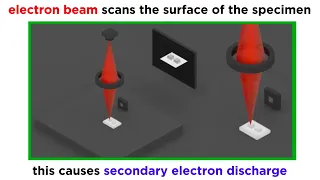
Electron microscopy techniques | Electron beam

Transmission electron microscopy

Transmission electron microscopy (TEM) is a microscopy technique in which a beam of electrons is transmitted through a specimen to form an image. The specimen is most often an ultrathin section less than 100 nm thick or a suspension on a grid. An image is formed from the interaction of the electrons with the sample as the beam is transmitted through the specimen. The image is then magnified and focused onto an imaging device, such as a fluorescent screen, a layer of photographic film, or a sensor such as a scintillator attached to a charge-coupled device. Transmission electron microscopes are capable of imaging at a significantly higher resolution than light microscopes, owing to the smaller de Broglie wavelength of electrons. This enables the instrument to capture fine detail—even as small as a single column of atoms, which is thousands of times smaller than a resolvable object seen in a light microscope. Transmission electron microscopy is a major analytical method in the physical, chemical and biological sciences. TEMs find application in cancer research, virology, and materials science as well as pollution, nanotechnology and semiconductor research, but also in other fields such as paleontology and palynology. TEM instruments have multiple operating modes including conventional imaging, scanning TEM imaging (STEM), diffraction, spectroscopy, and combinations of these. Even within conventional imaging, there are many fundamentally different ways that contrast is produced, called "image contrast mechanisms". Contrast can arise from position-to-position differences in the thickness or density ("mass-thickness contrast"), atomic number ("Z contrast", referring to the common abbreviation Z for atomic number), crystal structure or orientation ("crystallographic contrast" or "diffraction contrast"), the slight quantum-mechanical phase shifts that individual atoms produce in electrons that pass through them ("phase contrast"), the energy lost by electrons on passing through the sample ("spectrum imaging") and more. Each mechanism tells the user a different kind of information, depending not only on the contrast mechanism but on how the microscope is used—the settings of lenses, apertures, and detectors. What this means is that a TEM is capable of returning an extraordinary variety of nanometer- and atomic-resolution information, in ideal cases revealing not only where all the atoms are but what kinds of atoms they are and how they are bonded to each other. For this reason TEM is regarded as an essential tool for nanoscience in both biological and materials fields. The first TEM was demonstrated by Max Knoll and Ernst Ruska in 1931, with this group developing the first TEM with resolution greater than that of light in 1933 and the first commercial TEM in 1939. In 1986, Ruska was awarded the Nobel Prize in physics for the development of transmission electron microscopy. (Wikipedia).

Transmission electron microscopy
Video thumbnail

Electron Microscopy (TEM and SEM)

We've talked a lot about light microscopy, but this technique has inherent limitations in resolution and magnification. The next paradigm in microscopy that emerged in the middle of the 20th century was electron microscopy. Because electrons have much shorter wavelengths than photons, elec

From playlist Microbiology/Infectious Diseases

Video thumbnail

DIY Scanning Electron Microscope - Overview

Today, I finally produced an image with my DIY scanning electron microscope. I've spent the last few months working on this project, and am encouraged by today's success. There is still a lot of work left to do in making the image higher resolution, and eliminating sources of noise, howe

From playlist Scanning Electron Microscope

Video thumbnail

Stimulated Emission Explained

https://www.patreon.com/edmundsj If you want to see more of these videos, or would like to say thanks for this one, the best way you can do that is by becoming a patron - see the link above :). And a huge thank you to all my existing patrons - you make these videos possible. In this video

From playlist Optoelectronic and Photonic Devices

Video thumbnail

Electron beam control in a scanning electron microscope

I describe electron beam optics and deflection as they are employed in scanning electron microscopy. http://web.jfet.org/vclk/ - Deflection amplifier http://www.johngineer.com/blog/?p=648 - CRT Christmas tree http://www.fei.com/ - FEI Company

From playlist Scanning Electron Microscope

Video thumbnail

LASER Recombination Sources

https://www.patreon.com/edmundsj If you want to see more of these videos, or would like to say thanks for this one, the best way you can do that is by becoming a patron - see the link above :). And a huge thank you to all my existing patrons - you make these videos possible. In this video

From playlist Optoelectronic and Photonic Devices

Video thumbnail

Mod-01 Lec-37 Transmission Electron Microscopy

Nanostructures and Nanomaterials: Characterization and Properties by Characterization and Properties by Dr. Kantesh Balani & Dr. Anandh Subramaniam,Department of Nanotechnology,IIT Kanpur.For more details on NPTEL visit http://nptel.ac.in.

From playlist IIT Kanpur: Nanostructures and Nanomaterials | CosmoLearning.org

Video thumbnail

Fluorescent microscopes are amazing!

Fluorescent microscopy was always one of my favorite parts of working with mammalian cells as it always made for spectacular images. There are a variety of techniques that make use of fluorescence microscopy, many of which are used regularly in the best labs in the world. But fluorescence

From playlist Biology and Genetics

Video thumbnail

Animation of Fermilab's Accelerator Complex

The 6,800-acre Fermilab site is home to a chain of particle accelerators that provide particle beams to numerous experiments and R&D programs. This 2-minute animation explains how the proton source provides the particles that get accelerated and travel through the accelerator complex at cl

From playlist Detectors and Accelerators

Video thumbnail

Mary Scott - Supervised and Unsupervised approaches for Electron Microscopy Data Analysis

Recorded 01 December 2022. Mary Scott of the University of California, Berkeley, presents "Supervised and Unsupervised approaches for Electron Microscopy Data Analysis" at IPAM's Multi-Modal Imaging with Deep Learning and Modeling Workshop. Abstract: Recently, materials science has undergo

From playlist 2022 Multi-Modal Imaging with Deep Learning and Modeling

Video thumbnail

Microscopes: optical vs SEM vs TEM vs AFM

In order to examine defects and imperfections in materials, we need microscopes capable of enhancing our vision beyond the human eye capability. To access the micro, nano, and atomic scales needed we must rely on different microscopes. The microscope options vary immensely in terms of cost

From playlist Materials Sciences 101 - Introduction to Materials Science & Engineering 2020

Video thumbnail

Peter Binev - Modeling in Electron Microscopy - IPAM at UCLA

Recorded 13 September 2022. Peter Binev of the University of South Carolina presents "Modeling in Electron Microscopy" at IPAM's Computational Microscopy Tutorials. Learn more online at: http://www.ipam.ucla.edu/programs/workshops/computational-microscopy-tutorials/?tab=schedule

From playlist Tutorials: Computational Microscopy 2022

Video thumbnail

ASU Founders’ Day 2023: Peter Buseck — Faculty Service Achievement Award

Peter Buseck, a world-renowned researcher in solid-state geochemistry and mineralogy, cosmochemistry and atmospheric geochemistry, and faculty member in the Arizona State University School of Molecular Sciences and School of Earth and Space Exploration, is the recipient of the 2023 Faculty

From playlist Founders' Day 2023

Video thumbnail

Sarah Haigh - Probing atomic behaviour in liquids with STEM : opportunities for machine learning

Recorded 30 November 2022. Sarah Haigh of the University of Manchester presents "Probing atomic behaviour in liquids with STEM : opportunities for machine learning" at IPAM's Multi-Modal Imaging with Deep Learning and Modeling Workshop. Learn more online at: http://www.ipam.ucla.edu/progra

From playlist 2022 Multi-Modal Imaging with Deep Learning and Modeling

Video thumbnail

Petar Petrov - Laser phase-contrast transmission electron microscopy & computational opportunities

Recorded 15 November 2022. Petar Petrov of the University of California, Berkeley, presents "Laser phase-contrast transmission electron microscopy and associated computational opportunities" at IPAM's Cryo-Electron Microscopy and Beyond Workshop. Abstract: A phase plate can provide optimum

From playlist 2022 Cryo-Electron Microscopy and Beyond

Video thumbnail

Polarization of Light: circularly polarized, linearly polarized, unpolarized light.

3D animations explaining circularly polarized, linearly polarized, and unpolarized electromagnetic waves.

From playlist Physics

Video thumbnail

Materialism Podcast Ep 10. Seeing with Electrons

The optical microscope was discovered in the 17th century and ever since has been a staple of scientific discovery. It uncovered germs and let humanity investigate the microscopic world. However, optical microscopes face a limit to their resolution since they rely on visible light. If mate

From playlist Materialism Podcast

Related pages

Liquid-Phase Electron Microscopy | Phase retrieval | Detectors for transmission electron microscopy | Focused ion beam | Numerical aperture | Projection-slice theorem | Electronvolt | Photon-Induced Near-field Electron Microscopy | Scanning confocal electron microscopy | Negative stain | CMOS | Immunogold labelling | Space group | Electron | Nanometre | Autocorrelation | Frequency domain | In situ electron microscopy | Isosurface | High-resolution transmission electron microscopy | Energy filtered transmission electron microscopy | Uranyl acetate | Scanning transmission electron microscopy | Low-voltage electron microscope | Electron diffraction | Multislice | Neutron | Pascal (unit) | Electron microscope | Annular dark-field imaging | Atomic number | Magnetic hysteresis | Osmium tetroxide | Stigmator | Wavelength